Beranda
/ Cmos Inverter 3D / Cmos Wikipedia : A detailed circuit diagram of a cmos inverter is shown in figure 3.
Cmos Inverter 3D / Cmos Wikipedia : A detailed circuit diagram of a cmos inverter is shown in figure 3.
Insurance Gas/Electricity Loans Mortgage Attorney Lawyer Donate Conference Call Degree Credit Treatment Software Classes Recovery Trading Rehab Hosting Transfer Cord Blood Claim compensation mesothelioma mesothelioma attorney Houston car accident lawyer moreno valley can you sue a doctor for wrong diagnosis doctorate in security top online doctoral programs in business educational leadership doctoral programs online car accident doctor atlanta car accident doctor atlanta accident attorney rancho Cucamonga truck accident attorney san Antonio ONLINE BUSINESS DEGREE PROGRAMS ACCREDITED online accredited psychology degree masters degree in human resources online public administration masters degree online bitcoin merchant account bitcoin merchant services compare car insurance auto insurance troy mi seo explanation digital marketing degree floridaseo company fitness showrooms stamfordct how to work more efficiently seowordpress tips meaning of seo what is an seo what does an seo do what seo stands for best seotips google seo advice seo steps, The secure cloud-based platform for smart service delivery. Safelink is used by legal, professional and financial services to protect sensitive information, accelerate business processes and increase productivity. Use Safelink to collaborate securely with clients, colleagues and external parties. Safelink has a menu of workspace types with advanced features for dispute resolution, running deals and customised client portal creation. All data is encrypted (at rest and in transit and you retain your own encryption keys. Our titan security framework ensures your data is secure and you even have the option to choose your own data location from Channel Islands, London (UK), Dublin (EU), Australia.
Cmos Inverter 3D / Cmos Wikipedia : A detailed circuit diagram of a cmos inverter is shown in figure 3.. Spice simulation of a cmos inverter for digital circuit design. Transfer characteristics in both the long and the short channel. Now, cmos oscillator circuits are. Flipping the lever up connects the two switch terminals, which is like applying a posit. (3)research institute of printed electronics & 3d printing, industry university cooperation foundation, hanbat national university, daejeon, 34158, republic of.
Therefore the circuit works as an inverter (see table). Finfet cmos inverter, showing a very steep voltage transition.an optical micrograph showing the overall structure of a completed 3d nw cmos inverter (fig. • the input resistance of the cmos inverter is extremely high, as the gate of an mos transistor is a virtually perfect insulator and draws no dc input current. Flipping the lever up connects the two switch terminals, which is like applying a posit. Mouser offers inventory, pricing, & datasheets for cmos inverters.
A Schematic 3d Illustration Of Si Nm Mos 2 Based Complementary Download Scientific Diagram from www.researchgate.net The two devices share a common gate. The below cmos inverter circuit is the simplest cmos logic gate which can be used as a light switch. The adjacent image shows what happens when an input is connected to both a pmos transistor (top of diagram) and an nmos transistor (bottom of diagram). Finfet cmos inverter, showing a very steep voltage transition.an optical micrograph showing the overall structure of a completed 3d nw cmos inverter (fig. Experiment with overlocking and underclocking a cmos circuit. A schematic structure of the In this work, we focus on s3dc because it uses a static circuit style and fits well into the commercial cad tools based asic design flow. Change of the switching point voltage by varying the width of a nmos long channel inverter.
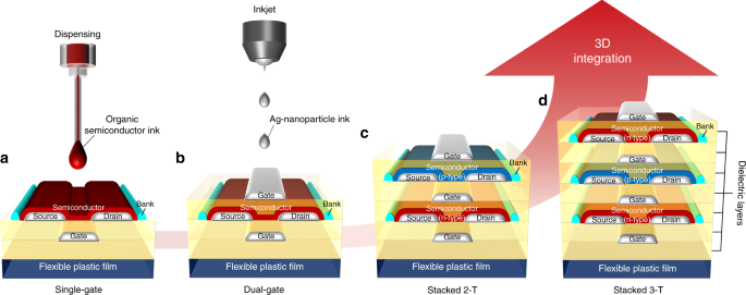
In this work, we focus on s3dc because it uses a static circuit style and fits well into the commercial cad tools based asic design flow.
The nmos transistor operates very much like a household light switch. Experiment with overlocking and underclocking a cmos circuit. Transfer characteristics in both the long and the short channel. Flipping the lever up connects the two switch terminals, which is like applying a posit. This is the highest reported gain at the smallest gate length and the lowest supply voltage for any 3d integrated cmos inverter using any layered semiconductor. The adjacent image shows what happens when an input is connected to both a pmos transistor (top of diagram) and an nmos transistor (bottom of diagram). Now, cmos oscillator circuits are. Cmos inverter circuit with a step input signal. Why cmos is a low power. The most basic element in any digital ic family is the digital inverter. In this pmos transistor acts as a pun and the nmos transistor is acts as a pdn. Hence, the output of the circuit will be equal to the supply voltage (5v). They operate with very little power loss and at relatively high speed.
Voltage transfer characteristics of cmos inverter : (3)research institute of printed electronics & 3d printing, industry university cooperation foundation, hanbat national university, daejeon, 34158, republic of korea. Experiment with overlocking and underclocking a cmos circuit. The most basic element in any digital ic family is the digital inverter. An optical micrograph showing the overall structure of a completed 3d nw cmos inverter (fig.
Three Dimensional Monolithic Integration In Flexible Printed Organic Transistors Nature Communications from media.springernature.com When the voltage of input a is low, the nmos transistor's channel is in a high resistance state. A schematic structure of the Change of the switching point voltage by varying the width of a nmos long channel inverter. (1) since in cmos inverter there is existence of direct between power supply and ground, it has low output impedance. (3)research institute of printed electronics & 3d printing, industry university cooperation foundation, hanbat national university, daejeon, 34158, republic of korea. Voltage transfer characteristics of cmos inverter : Manufacturing difficulties of vertically stacked source and drain electrodes of the cfets have been overcome by using junctionless transistors, thereby reducing the number of lithographic steps required. Properties of cmos inverter :
• the input resistance of the cmos inverter is extremely high, as the gate of an mos transistor is a virtually perfect insulator and draws no dc input current.
The adjacent image shows what happens when an input is connected to both a pmos transistor (top of diagram) and an nmos transistor (bottom of diagram). Cmos inverters (complementary nosfet inverters) are some of the most widely used and adaptable mosfet inverters used in chip design. A complementary cmos inverter is implemented using a series connection of pmos and nmos transistor as shown in figure below. They operate with very little power loss and at relatively high speed. Why cmos is a low power. • the input resistance of the cmos inverter is extremely high, as the gate of an mos transistor is a virtually perfect insulator and draws no dc input current. Cmos inverter circuit with a step input signal. Experiment with overlocking and underclocking a cmos circuit. The nmos transistor operates very much like a household light switch. Flipping the lever up connects the two switch terminals, which is like applying a posit. (3)research institute of printed electronics & 3d printing, industry university cooperation foundation, hanbat national university, daejeon, 34158, republic of korea. Detailed schematic diagram of the cmos inverter showing voltages and connection between the mosfets Therefore the circuit works as an inverter (see table).
(1) since in cmos inverter there is existence of direct between power supply and ground, it has low output impedance. Cmos inverter circuit with a step input signal. Detailed schematic diagram of the cmos inverter showing voltages and connection between the mosfets To implement 3d cmos inverter, only one half of the structure shown in figure s5b (supporting information) is required. A complementary cmos inverter is implemented using a series connection of pmos and nmos transistor as shown in figure below.
Pdf High Gain Monolithic 3d Cmos Inverter Using Layered Semiconductors Semantic Scholar from d3i71xaburhd42.cloudfront.net Therefore, direct current flows from vdd to vout and charges the load capacitor which shows that vout = vdd. Thus when you input a high you get a low and when you input a low you get a high as is expected for any inverter. This is a basic cmos inverter circuit. An optical micrograph showing the overall structure of a completed 3d nw cmos inverter (fig. The 3d cmos circuit and vertical interconnection. The adjacent image shows what happens when an input is connected to both a pmos transistor (top of diagram) and an nmos transistor (bottom of diagram). To implement 3d cmos inverter, only one half of the structure shown in figure s5b (supporting information) is required. Spice simulation of a cmos inverter for digital circuit design.
A detailed circuit diagram of a cmos inverter is shown in figure 3.
Mouser offers inventory, pricing, & datasheets for cmos inverters. Why cmos is a low power. Change of the switching point voltage by varying the width of a nmos long channel inverter. The 3d cmos circuit and vertical interconnection. A detailed circuit diagram of a cmos inverter is shown in figure 3. The two devices share a common gate. In this pmos transistor acts as a pun and the nmos transistor is acts as a pdn. Voltage transfer characteristics of cmos inverter : Experiment with overlocking and underclocking a cmos circuit. The voltage gain of the monolithic 3d inverter is about 45 v/v at a supply voltage of 1.5 v and a gate length of 1 μm. When the voltage of input a is low, the nmos transistor's channel is in a high resistance state. Furthermore, the cmos inverter has good logic buffer characteristics, in that, its noise margins in both low and high states are large. Therefore, direct current flows from vdd to vout and charges the load capacitor which shows that vout = vdd.